



NPN Transistors 2SC2412
NPN Transistors 2SC2412 are categories based on the layering of the semi conductive materials. NPN transistors contain negative, positive, and negative layers while PNP transistors contain positive, negative, and positive layers. But the purpose of the transistor (an electrical switch or amplifier) is essentially the same.
Description
Professional Technical Team
The top management of our company has two professors from electric university of Zhejiang university, and we have employed several aerospace and military project level power supply research and develop specialists in 2011, and we found TRR micro power supply research institute, we are professionally design and modify the power supply product scheme for customers, save cost and improve energy efficiency, or replace the lacked IC.
Rich Experience
TRR shares has multiply areas core technologies in wafer, package, apparatus test and application design, etc, we devote into research, manufacture, sell and application scheme design in new type components, already obtained more than 80 national authorized invent patents, include the general MB10F bridge in power supply industry, LED industry used UMB10F / B7 bridge, the globe smallest bridge IBS and series high junction temperature products.
Wide Product Range
Our company focus on that provide the industry commonly used and customized products and service according to requirements for the users, the products widely applied in many areas such as power supply and adapters (customer: SUNGROW power supply), green lighting (customers: MLS, TOSPO lighting), router (customer: Huawei), smart phone (customers: Huawei, Xiaomi, OPPO) and communication products, automobile electrics (customer: SAIC General Motors), frequency transformer, big and small household electrical appliances (customer: Gree), safety guard area (HIKVISION, DAHUA) and other areas.
NPN Transistors 2SC2412 are categories based on the layering of the semi conductive materials. NPN transistors contain negative, positive, and negative layers while PNP transistors contain positive, negative, and positive layers. But the purpose of the transistor (an electrical switch or amplifier) is essentially the same.

The Transistor 2SA733 is a high-performance, stable, and low saturation voltage semiconductor device made of epitaxial nnp jet silicon material, which has a wide range of applications. This product has been widely used in various fields such as automatic control systems, amplifier circuits, switch circuits, power management, and communication electronics.
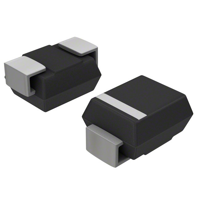
SURFACE MOUNT SILICON RECTIFIER 2A1
SURFACE MONT SILICON RECTIFIER 2A1, as an electronic component, has the advantages of small size, light weight, space saving, good electrical performance, high power, high stability, and long service life, and can be widely used in various fields.

TO-126 Plastic-Encapsulate Transistors 13003
TO-126 Plastic Encapsulate Transistors 13003 is an NPN transistor commonly used in electronic circuits. It can be used in various circuits and has high power amplification and switching effects. Suitable for various household appliances, electronic instruments, electronic products, automotive electronics, computer peripherals, etc.


Benefits of NPN Transistors 2SC2412
An NPN Transistors 2SC2412 is a type of bipolar junction transistor (BJT). It consists of a layer of p-type semiconductor material sandwiched between two layers of n-type semiconductor material. The two n-type layers act as the emitter and collector, and the p-type layer acts as the base. The transistor is called NPN because the majority of carriers in the emitter and collector regions are electrons, which are negatively charged.
The advantages of NPN Transistors 2SC2412 are shown below:
· High gain and high input impedance
· Low noise
· Fast switching speed
· Low cost
· Easy availability
A NPN Transistors 2SC2412 Configuration
The construction and terminal voltages for a NPN Transistors 2SC2412 are shown above. The voltage between the Base and Emitter ( VBE ), is positive at the Base and negative at the Emitter because for an NPN transistor, the Base terminal is always positive with respect to the Emitter. The Collector supply voltage must also be more positive with respect to the Emitter ( VCE ).
Therefore, for a bipolar NPN transistor to conduct correctly, the Collector must always more positive with respect to both the Base and the Emitter terminals.
Then the voltage sources are connected to an NPN transistor as shown. The Collector is connected to the supply voltage VCC via the load resistor, RL which also acts to limit the maximum current flowing through the device.
The Base supply voltage VB is connected to the Base resistor RB, which again is used to limit the maximum Base current.
So in a NPN Transistors 2SC2412 it is the movement of negative current carriers (electrons) through the Base region that constitutes transistor action, since these mobile electrons provide the link between the Collector and Emitter circuits. This link between the input and output circuits is the main feature of transistor action because the transistors amplifying properties come from the consequent control which the Base exerts upon the Collector to Emitter current.
Then we can see that the transistor is a current operated device (Beta model) and that a large current ( Ic ) flows freely through the device between the collector and the emitter terminals when the transistor is switched "fully-ON". However, this only happens when a small biasing current ( Ib ) is flowing into the base terminal of the transistor at the same time thus allowing the Base to act as a sort of current control input.
The current in a bipolar NPN transistor is the ratio of these two currents ( Ic/Ib ), called the DC Current Gain of the device and is given the symbol of hfe or nowadays Beta, ( β ).
The value of β can be large up to 200 for standard transistors, and it is this large ratio between Ic and Ib that makes the bipolar NPN transistor a useful amplifying device when used in its active region as Ib provides the input and Ic provides the output. Note that Beta has no units as it is a ratio.
Also, the current gain of the transistor from the Collector terminal to the Emitter terminal, Ic/Ie, is called Alpha, ( α ), and is a function of the transistor itself (electrons diffusing across the junction).
As the emitter current Ie is the sum of a very small base current plus a very large collector current, the value of alpha (α), is very close to unity, and for a typical low-power signal transistor this value ranges from about 0.950 to 0.999.
Working Principle of NPN Transistors 2SC2412
The working principle of an NPN Transistors 2SC2412 is based on the control of current flow between the emitter and collector regions by varying the base current. The NPN transistor has three terminals: the emitter (E), the base (B), and the collector (C). The emitter is made of N-type material, the base is made of P-type material, and the collector is made of N-type material.
When a small positive voltage is applied to the base-emitter junction, the junction becomes forward-biased, allowing electrons to flow from the emitter to the base. Since the base region is thin and lightly doped, only a small fraction of these electrons recombine with holes in the base. The majority of the electrons continue to flow through the base and reach the collector, which is reverse-biased.
The reverse-biased base-collector junction creates an electric field that repels the electrons away from the base and attracts them toward the collector. As a result, a large current flows from the collector to the emitter, which is controlled by the smaller base current. The ratio of the collector current to the base current is known as the current gain (β) of the transistor.
Transistors with NPN Diodes (NPN) are used in a variety:
· High-frequency applications make use of these.
· Switching applications are where NPN transistors are most commonly used.
· This component is used in amplifying circuits.
· To amplify weak signals, it's used in Darlington pair circuits.
· NPN transistors are used in applications where a current sink is required.
· Some classic amplifier circuits, such as 'push-pull' amplifier circuits, make use of this component.
· In temperature sensors, for example.
· Applications with extremely high frequency.
· In logarithmic converters, this variable is used.
· Because signal amplification is done with NPN transistors. In amplifying circuits, it is used in this way.
· Logarithmic converters are another area where it is used.
· The switching characteristic of the NPN transistor is one of its most significant advantages. As a result, it's commonly used in switching applications.

Construction of NPN Transistors 2SC2412
The NPN transistor is constructed with two diodes that are connected in such a way that their backs get connected to one another. These diodes are connected in such a way that the three terminals are formed known as collector base and emitter. Two junctions are formed in it-one is emitter-base and the other is collector base.
The NPN transistor is created when 3 layers are combined, namely-two N-type semiconductors, and one P-type semiconductor in the middle. Two diodes are connected together, which results in four doped regions as each of the diodes has 2 doped regions. The base that is created will not have uniform doping.
Hence, an NPN transistor is always built in three layers, of which, the base is lightly doped, the emitter is heavily doped and the collector is moderately doped. The base of the P-type semiconductor is set up at the centre, between the emitter and the collector of the N-type semiconductor.
The transistor operates on different modes or regions depends on the biasing of junctions. It has three modes of operation.
Cut-Off Mode
In cur-off mode, both junctions are in reverse bias. In this mode, the transistor behaves as an open circuit. And it will not allow the current to flow through the device.
Saturation Mode
In the saturation mode of a transistor, both junctions are connected in forward bias. The transistor behaves as a close circuit and current flow from collector to emitter when the base-emitter voltage is high.
Active Mode
In this mode of a transistor, the base-emitter junction is forward bias and collector-base junction is reverse biased. In this mode, the transistor operates as a current amplifier.
The current flows between emitter and collector and the amount of current are proportional to the base current.
NPN Transistors 2SC2412: How Do You Know If a Transistor is NPN or PNP?
Arrow Orientation on Schematic Symbol
The schematic symbols for NPN and PNP transistors are similar, but the orientation of the arrow on the emitter indicates the transistor type. In an NPN transistor symbol, the arrow points outward from the base, while in a PNP transistor symbol, the arrow points inward toward the base.
Polarity Test
Using a multimeter in diode test mode, you can determine the polarity of the transistor junctions. For an NPN transistor, the base-emitter junction will show a forward bias (low resistance) when the positive probe is connected to the base and the negative probe to the emitter. The base-collector junction will show a reverse bias (high resistance). In contrast, for a PNP transistor, the base-emitter junction will show a forward bias when the negative probe is connected to the base and the positive probe to the emitter, while the base-collector junction will show a reverse bias.
Collector-Base Breakdown Voltage
NPN Transistors 2SC2412 typically have a higher collector-base breakdown voltage compared to their emitter-base breakdown voltage, while PNP transistors have a higher emitter-base breakdown voltage compared to their collector-base breakdown voltage. Measuring these breakdown voltages can help identify the transistor type.
Our Factory
TRR Electronics Co.,Ltd is one state capital hold controlling interest enterprise which make research, develop, manufacture and sell semiconductor discrete components and products as main operating business. We are subsidiary of A-shares quoted company 600059 and found in 2000,Toexpand oversea market business, Established subsidiary Guangdong TRR Electronics Co., Ltd.
TRR shares has multiply areas core technologies in wafer, package, apparatus test and application design, etc, we devote into research, manufacture, sell and application scheme design in new type components, already obtained more than 80 national authorized invent patents, include the general MB10F bridge in power supply industry, LED industry used UMB10F / B7 bridge, the globe smallest bridge IBS and series high junction temperature products.

Our Certificate


Ultimate FAQ Guide to NPN Transistors 2SC2412
Hot Tags: npn transistors 2sc2412, China, suppliers, manufacturers, factory, distributors, quotation, inventory, Shenzhen, OEM, in stock
Send Inquiry
You Might Also Like


