What should be noted in the layout design of medical device diodes?
Leave a message
1, Polarity identification and error prevention design
A diode has unidirectional conductivity, and reversing its polarity may cause a short circuit or burn out the device. In medical equipment, this error may cause equipment failure and even harm to patients. Therefore, the layout design must strictly follow the following principles:
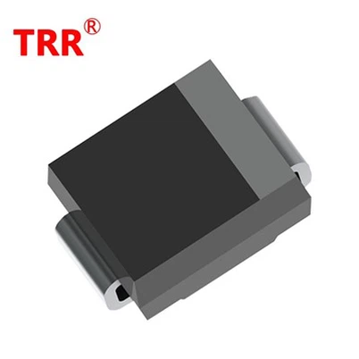
Silk screen marking: Clearly mark the cathode (K) or negative electrode (-) around the diode body, commonly represented by vertical lines, thick lines, notch markings, or the letter "K". For example, surface mount diodes can correspond to cathodes through color bands or grooves.
Packaging correspondence: PCB packaging pads need to be clearly distinguished between cathode/anode. Typically, cathode pads are designed with notches, corners, or special shapes to avoid welding errors.
Direction uniformity: The same type of diode should maintain the same direction (such as all cathodes facing left/up) to reduce the risk of welding errors.
Anti mistake design: For critical circuits or error prone situations, asymmetric pad design can be used to further prevent polarity reversal.
2, Heat dissipation design and thermal management
In medical equipment, power diodes (such as rectifiers and freewheeling tubes) generate significant heat during operation. Poor heat dissipation may lead to thermal breakdown or performance degradation. Layout design needs to optimize heat dissipation from the following aspects:
Approaching the heat dissipation source: Place the power diode near the heat sink or copper foil area, and use metal conductors to quickly conduct heat. For example, in the power module of portable ultrasound devices, silicon carbide diodes are in close contact with the heat sink through thermal pads to reduce junction temperature.
Large area copper plating: Connect a large area of ground copper foil (GND Plane) or power copper foil to the cathode and anode pads of the diode to enhance heat dissipation capability. For example, in the electrode detection circuit of an electrocardiograph, multiple layers of copper foil are laid under the voltage regulator diode pad and connected to the inner heat dissipation layer through vias.
Heat dissipation via: densely arrange heat dissipation via holes (diameter 0.3mm, spacing 0.5-1mm) in the area where large copper foils are connected, forming a low thermal resistance path. For example, in the power conversion circuit of portable X-ray equipment, a grid like via array is used below the silicon carbide diode, reducing temperature rise by 40%.
Stay away from heat sensitive components: Avoid placing heating diodes in close proximity to heat sensitive components such as electrolytic capacitors and precision ICs to prevent performance degradation caused by thermal stress.
3, Electrical isolation and safety regulations requirements
Medical equipment must meet strict electrical safety standards (such as IEC 60601-1), and the diode layout must ensure isolation between high and low voltage areas to prevent the risk of electric shock
Creepage distance and electrical clearance: Adequate spacing should be maintained between the pins of high-voltage diodes (such as those above 600V) and other high-voltage devices/wiring. For example, in the high-voltage generation circuit of a defibrillator, a creepage distance of at least 2mm is set between the diode and the capacitor, and insulation strength is increased by opening windows.
Isolation groove and window: Between high and low voltage areas, windows can be opened under the solder mask layer (copper free area), and even slots can be made on the PCB to increase the creepage distance. For example, in the power module of medical laser equipment, the high voltage side and low voltage side are completely separated by isolation slots.
Power ground and signal ground separation: physically separate the power ground (PGND) carrying large pulse currents from the signal ground (SGND) that requires quietness, and connect them at a single point to avoid interference. For example, in the signal acquisition circuit of a portable monitor, the ground wire of the photodiode is independently wired from the power ground to reduce noise coupling.
4, EMI suppression and high-frequency optimization
In medical equipment, the high-frequency switching action of diodes may generate electromagnetic interference (EMI), affecting equipment performance or interfering with other medical devices. Layout design needs to suppress EMI from the following aspects:
Minimize critical loop area: Compact the layout of high-frequency switching loop components such as diodes, switching tubes, energy storage inductors/capacitors, etc., and shorten the routing length. For example, in Buck/Boost circuits, the freewheeling diode is placed adjacent to the switching transistor, forming a triangular layout to reduce the loop area.
Parasitic parameter control: In high-frequency applications, the parasitic capacitance (Cj) and inductance (Ls) of diodes can cause signal attenuation or ringing. Low capacitance diodes (such as Schottky diodes) should be selected, and current crowding effects should be reduced by optimizing wiring (such as 45 degree or rounded corners).
Shielding and filtering: Ground isolation or differential routing is used for sensitive signal lines (such as I2C, SPI), and ferrite beads or filtering capacitors are added at the input/output terminals. For example, in the communication interface of portable blood glucose meters, TVS diodes are combined with common mode inductors to suppress ESD and conducted interference.
5, Protection layout and reliability design
Medical equipment needs to have high reliability, and diode layout should consider protective measures such as overvoltage, overcurrent, ESD, etc.:
Overvoltage protection: Use a Zener diode or TVS diode at the power input to clamp the voltage and prevent voltage spikes from damaging the secondary circuit. For example, in the power module of a portable oxygen concentrator, the TVS diode is connected in parallel at the input end, with a response time of less than 1ps, and can withstand 8kV contact discharge.
Overcurrent protection: The current is limited by a series resistor or current limiting diode to prevent the diode from burning out due to overload. For example, in a light-emitting diode (LED) driver circuit, a current limiting resistor is connected in series with the LED to ensure that the operating current is within a safe range.
ESD protection: Install ESD diodes near data interfaces (such as USB and Ethernet ports) and follow the principle of "close to ESD inlet". For example, in the USB interface of portable ultrasound devices, the distance between the TVS diode and the connector is less than 3cm, and the ground terminal is connected to the ground plane through multiple vias, resulting in a 15V decrease in clamping voltage.
6, Layout optimization for special application scenarios
For the special needs of medical equipment, the diode layout needs to be further optimized:
Flexible circuit design: In wearable medical devices such as smart dressings, diodes need to be connected through flexible power wiring to adapt to device deformation. For example, light-emitting diodes are connected to sensor substrates through flexible PCBs, and even if the thickness of the dressing changes, the LEDs can still be stably arranged on the surface to avoid compressing the patient's affected area.
Low power design: In portable devices, choose low leakage current diodes (such as ultrafast recovery diodes) to reduce static power consumption. For example, in the signal acquisition circuit of portable electrocardiogram monitors, photodiodes are designed with low dark current and paired with low-noise operational amplifiers to improve the signal-to-noise ratio.
High density integration: In micro medical devices such as implantable sensors, miniaturized packaged diodes (such as DFN, SOD-123) are used to save space. For example, in the power management circuit of neural stimulators, silicon carbide diodes are packaged in DFN, which reduces the area by 80% compared to traditional TO-220 packaging.