How to improve the safety of consumer electronic devices through diodes?
Leave a message
1, The mechanism of diodes in the safety protection of consumer electronic devices
1. Anti static protection
Principle: The transient high voltage generated by ESD events may breakdown electronic components, leading to equipment failure. Through its nonlinear volt ampere characteristics, diodes quickly conduct during ESD surges, bypassing electrostatic charges to ground and protecting sensitive circuits.
Implementation method:
TVS diode: With low clamping voltage and fast response time (usually<1s), it is suitable for ESD protection of high-speed interfaces such as USB and HDMI.
ESD protection diode array: integrates multiple diodes to provide multi-channel protection, suitable for portable devices such as mobile phones and tablets.
Case: A certain smartphone manufacturer uses a bidirectional TVS diode at the USB interface to bypass the ESD surge current to ground, enabling the device to pass the IEC 61000-4-2 8kV contact discharge test and reduce the failure rate by 90%.
2. Overvoltage protection
Principle: Fluctuations in power supply voltage or lightning strikes may cause transient overvoltage at the input of the device. Zener diodes can clamp the voltage within a safe range during reverse breakdown, preventing damage to the subsequent circuit.
Implementation method:
Transient Voltage Suppression (TVS) diode: suitable for overvoltage protection of power and signal lines.
Gas discharge tube (GDT) and diode combination: GDT handles high-energy surges, while diodes handle low-energy transients, forming multi-level protection.
Case: A certain network router uses a combination of TVS diode and GDT at the power input end. During the IEC 61000-4-5 4kV surge test, the device maintained normal operation without hardware damage.
3. Electromagnetic compatibility (EMC) optimization
Principle: The nonlinear characteristics of diodes can absorb or reflect electromagnetic interference (EMI) signals, reduce the radiation interference of equipment to the outside world, and enhance anti-interference ability.
Implementation method:
Schottky diode: low forward voltage drop and fast switching characteristics, suitable for EMI filtering in high-frequency circuits.
Variable capacitance diode: By adjusting the capacitance value, the resonant frequency of the RF circuit is optimized to reduce EMI.
Case: A smart wearable device uses Schottky diodes for EMI filtering in its Bluetooth module, enabling the radiated interference test (CISPR 32) to pass Class B standards and reduce interference with other devices.
2, The specific application of diodes in consumer electronic devices
1. Smartphones
Application scenarios:
USB interface: Bidirectional TVS diode to prevent ESD shock.
Camera module: Zener diode protects the image sensor from power fluctuations.
RF front-end: Schottky diode for bias control of low-noise amplifier.
Optimization measures:
Using small-sized diodes packaged in 0201 to save PCB space.
Combining EMC simulation tools to optimize diode layout and reduce antenna coupling effects.
2. Tablet computer
Application scenarios:
Power adapter interface: Multi stage TVS diodes combined with GDT provide comprehensive overvoltage protection.
Display backlight driver: Zener diode ensures stable LED driving current and extends service life.
Touch panel: ESD protection diode array to prevent human static interference.
Optimization measures:
Use low capacitance TVS diodes (<1pF) to reduce attenuation of high-speed signals.
Adopting a system level ESD protection strategy, combined with software algorithms to achieve real-time monitoring.
3. Smart wearable devices
Application scenarios:
Heart rate sensor: A voltage regulator diode protects sensitive circuits from power noise interference.
Wireless charging module: TVS diode prevents overvoltage events during the charging process.
Flexible Circuit Board (FPC): Ultra small ESD protection diode array, suitable for small spaces.
Optimization measures:
Develop customized diode packaging to meet the bending requirements of flexible circuits.
Combining low-power design, choose ESD protection devices with low leakage current.
3, Diode selection and layout optimization
1. Key selection points
Voltage level: Select the appropriate reverse breakdown voltage (VBR) based on the operating voltage of the circuit.
Capacitance value: Low capacitance diodes should be selected for high-speed signal lines to avoid signal distortion.
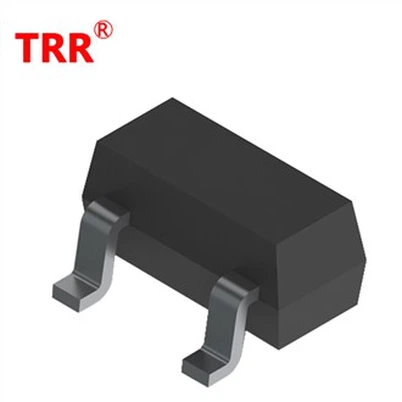
Packaging form: Select small packages such as SOT-23 and DFN based on PCB space and heat dissipation requirements.
2. Layout optimization
Approaching the protection point: The diode should be as close as possible to the protected circuit to reduce parasitic inductance.
Ground plane treatment: Ensure that the ground pin of the diode is well connected to the ground plane to reduce the ground bounce effect.
Thermal management: In high-frequency or high current applications, it is necessary to reduce the temperature of diodes through heat sinks or PCB heat dissipation layers.
https://www.trrsemicon.com/diode/smd-diode/bzt52c2v4-c43.html