How to choose Schottky diodes for wearable medical devices?
Leave a message
1, Core parameters: Accurately matching the low power consumption and miniaturization requirements of wearable devices
1. Forward voltage drop (VF): determines power conversion efficiency
The forward voltage drop of Schottky diodes directly affects the power consumption of circuits. For example, in 5V power rectification, if SR360 (3A/60V) with VF=0.4V is used, the efficiency can be improved by 5%, saving nearly 50% of heat generation compared to silicon tubes. For wearable devices such as smart bracelets and blood glucose meters, their battery capacity is usually between 100-500mAh, and low VF diodes can significantly extend the battery life. Taking the heart rate monitoring module as an example, if SS14F (1A/40V) with VF=0.3V is used, compared to silicon tubes with VF=0.7V, the power consumption is reduced by 57%, and the single charge usage time is nearly doubled.
2. Reverse leakage current (IR): affecting the reliability of low-power design
The reverse leakage current increases exponentially with temperature, which may cause circuit false triggering or battery self discharge in high temperature environments (such as when worn by the human body). For example, BAT54S (0.2A/30V) has an IR of 5 μ A at 25 ℃, but may rise above 100 μ A at 85 ℃. For ECG devices that require long-term monitoring, using diodes with high IR may cause sensor baseline drift and affect data accuracy. Therefore, low IR models (such as RB531XN, IR)= 0.03mA@10V )More suitable for power sensitive scenarios.
3. Reverse Voltage Endurance (VR): Ensuring circuit safety margin
Wearable devices typically use low voltage power supplies (3.3V-5V), but transient voltage surges (such as electrostatic discharge or power fluctuations) need to be considered. For example, in the USB PD fast charging interface, the MBR3045PT (30A/45V) can withstand 12V/3A output with a heat loss of only 1.2W, making it suitable for miniaturized heat dissipation design. For medical grade equipment (such as insulin pumps), it is necessary to choose a model with VR ≥ 2 times the working voltage (such as SS56, 5A/60V, VR=60V) to avoid voltage spikes damaging the circuit.
4. Packaging size and thermal resistance: balancing performance and space limitations
Wearable devices are extremely sensitive to PCB area and thickness. For example, Dior's SDT2U60CP3 uses the X3-DSN1406-2 package, which is only 3.4% the size of traditional SMB packages, reduces weight by 99%, and achieves low loss with VF=0.51V. For high-density designs such as smart earplugs, the SMAF package (such as SS14F) has a thickness of only 0.5mm and can be directly mounted on a flexible circuit board (FPC), saving space while optimizing the heat dissipation path.
2, Application scenario adaptation: differentiated selection from power management to signal protection
1. Power management: efficient rectification and continuous current
Switching power supply (DC-DC converter): Choose a model with low VF and short reverse recovery time (trr). For example, the OBC charger for new energy vehicles uses MBR20100CT (20A/100V), which reduces high-frequency rectification losses by 40% and supports switching frequencies above 100kHz, reducing the size of the inductor. In wearable devices, similar technologies can be applied to wireless charging modules to improve energy conversion efficiency.
Lithium battery protection circuit: It needs to withstand high current pulses (such as charging overcurrent protection). The SBR10U30CT (10A/30V) adopts a trench structure with a surge current capacity of 40A, which is suitable for protecting lithium battery packs from short-circuit impact.
2. Signal detection: low noise and high sensitivity
Bioelectric signal acquisition (ECG/EEG): Low junction capacitance (Cj) and low IR models should be selected to reduce signal distortion. For example, BAT46WS (0.15A/100V) with Cj=2pF at 1MHz can effectively suppress high-frequency noise and improve the signal-to-noise ratio of electrocardiogram signals.
Optical sensor (blood oxygen/heart rate): needs to be matched with LED driver circuit. For example, in the driving of green LED (520nm), using a Schottky diode with VF=0.3V can reduce the driving voltage and extend the lifespan of the LED.
3. Protection circuit: anti reverse connection and ESD protection
Input anti reverse connection: Select a model with VR ≥ 2 times the input voltage. For example, in a 5V input circuit, using SS12 (1A/40V) can prevent diode breakdown when the power supply is reversed, and the voltage drop of VF=0.55V has little impact on the circuit.
ESD protection: It needs to be used in conjunction with TVS diodes. For example, in the USB interface, using SMBJ5.0CA (5V TVS) in parallel with SS14F (1A/40V) can withstand 8kV contact discharge and protect the downstream circuit.
3, Selection Practice: From Parameter Comparison to Supply Chain Optimization
1. Parameter Comparison Table: Performance Analysis of Typical Models
Model VF (@ 1A) IR (@ 25 ℃) VR (V) Packaging Application Scenarios
SS14F 0.55V 300 μ A 40V SMAF power rectifier, anti reverse connection
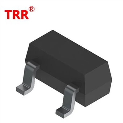
BAT54S 0.3V 5 μ A 30V SOT-23 signal detection, low-power circuit
MBR20100CT 0.4V 1mA 100V TO-220 High Voltage Rectification, Motor Drive
SDT2U60CP3 0.51V 10 μ A 60V X3-DSN1406-2 ultra compact equipment
2. Supply Chain Optimization: Balancing Cost and Reliability
Vehicle level certification: For medical grade equipment (such as implantable sensors), it is necessary to choose a model that has passed AEC-Q101 certification (such as SK34L, 3A/40V) to ensure stable operation in an environment of -40 ℃ to 150 ℃.
Multi source supply: Avoiding the risk of a single supplier. For example, SS14F is produced by multiple manufacturers such as Heketai and Ansenmei, and can flexibly switch supply chains.
Lifecycle management: Prioritize the selection of mature models (such as 1N5819, 1A/40V) to avoid design changes due to production stoppage.