How to address the challenge of high-frequency diodes in the energy system?
Leave a message
一, The core pain points of high-frequency challenges
1. Electromagnetic interference (EMI) loss of control
The high-frequency switching action (such as the di/dt of SiC MOSFET reaching 10 ³ -10 ⁴ A/μ s) will produce steep voltage spikes (dv/dt>10kV/μ s), resulting in significantly enhanced conduction and radiation interference. For example, in photovoltaic inverters, high-frequency noise may interfere with the voltage monitoring system of the power grid, causing data acquisition errors exceeding 5%; In 5G base stations, the EMI spectrum extends beyond 30MHz, which is beyond the suppression range of traditional LC filters. Multi order π - type filters need to be designed, but it will increase additional losses by 2-3%.
2. Sudden increase in thermal management pressure
High frequency increases the power density to over 15kW/L, resulting in a significant increase in heat generation per unit volume. Taking the drive inverter of new energy vehicles as an example, the junction temperature of SiC diodes needs to be controlled below 125 ℃ under high-frequency operation, and the traditional air-cooled heat dissipation efficiency is insufficient (≤ 50W/(m ² · K)), requiring the use of a liquid cooling+heat pipe composite system, but it will increase equipment weight and cost. In addition, high-frequency transformers are prone to local winding temperatures exceeding 150 ℃ due to skin and proximity effects, further exacerbating the risk of thermal runaway.
3. Material performance and packaging bottleneck
Traditional silicon-based materials approach their physical limits at high frequencies: the reverse recovery time (TRR) of silicon diodes can reach tens to hundreds of nanoseconds, resulting in switch losses accounting for over 30%; The iron loss of silicon steel sheet transformers at 100kHz is more than 100 times that of the power frequency, requiring the use of high-frequency magnetic core materials such as nanocrystalline alloys, but the cost is high (5-8 times that of silicon steel sheets). In terms of packaging, traditional TO-247 packaging exhibits significant parasitic inductance above 100kHz, requiring a switch to flip chip or planar packaging. However, the heat dissipation path is complex and the cost increases by 20-30%.
二, Technological breakthrough: full chain optimization from devices to systems
1. Application of new semiconductor materials
Silicon carbide (SiC) diode: The bandgap width of SiC material is three times that of silicon, the breakdown electric field strength reaches 2-3MV/cm, and the reverse recovery time can be shortened to several tens of nanoseconds. In photovoltaic inverters, SiC diodes reduce switching losses by 30% and achieve conversion efficiency exceeding 98%; In the drive inverter of new energy vehicles, its high temperature stability (junction temperature up to 200 ℃) supports 800V high-voltage platform, and the radiator volume is reduced by 40%.
Gallium Nitride (GaN) Diode: GaN has an electron mobility of 2000cm ²/(V · s), making it suitable for RF and high-frequency applications. In the millimeter wave front end of 5G base stations, GaN diodes achieve efficient signal rectification and detection, reducing power consumption by 30% compared to silicon devices, and supporting stable operation in the 24GHz-52GHz frequency band.
Two dimensional material diode: Graphene diode utilizes zero bandgap characteristics to achieve high-speed switching in the terahertz (THz) frequency band, providing core components for 6G communication pre research; MoS ₂ diodes achieve programmable rectification characteristics through heterojunction structures, replacing multiple functional devices in reconfigurable computing chips and improving integration and energy efficiency.
2. Innovation in packaging technology
Three dimensional vertical structure: By using deep trench etching and epitaxial growth techniques, the current transmission path is transformed from horizontal to vertical, increasing the current density to over 200A/cm ². Vertical SiC PiN diodes can withstand thousands of volts of reverse voltage in high-voltage direct current transmission (HVDC) systems, reducing the number of converter station components and system losses.
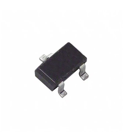
Surface mount technology (SMT) and flip chip technology: SMT packaging increases the contact area between diodes and circuit boards, improving heat dissipation efficiency by 40%; Inverted chip technology shortens the connection distance between chips and circuit boards, reduces signal transmission losses and thermal resistance, and is suitable for high-frequency and high current scenarios in high-end electronic devices.
Low parasitic parameter packaging: Using low inductance bonding wires and low capacitance substrate materials to reduce the impact of packaging parasitic parameters on high-frequency performance. For example, the parasitic inductance of SiC module packaging developed by a certain enterprise is as low as 2nH, and it supports increasing the switching frequency to above 1MHz.
三, System Optimization: Collaborative Innovation from Design to Operations
1. EMI suppression and electromagnetic compatibility (EMC) design
Multi order filtering and shielding technology: In photovoltaic inverters, a combination of π - type filters and common mode chokes is used to suppress high-frequency noise above 30MHz; In new energy vehicle charging stations, shielding copper foil and metal covers are used to reduce electromagnetic radiation and meet CISPR 32 standards.
Soft switching technology: By using zero voltage switching (ZVS) or zero current switching (ZCS) to reduce di/dt and dv/dt, reverse recovery losses are minimized. For example, after applying soft switching technology to a certain power electronic device, the overall energy consumption of the system decreased by more than 25%.
AI driven dynamic EMI management: using machine learning models to analyze historical operating data, predict current fluctuations, and optimize diode control strategies. For example, a certain patent scheme uses neural networks to adjust the conduction timing in real time, reducing EMI noise by 15dB.
2. Intelligent upgrade of thermal management system
Liquid cooling and phase change material (PCM) composite heat dissipation: In the power system of data centers, a heat dissipation scheme of liquid cooling plate+PCM filling is adopted to stabilize the junction temperature of SiC diodes below 125 ℃ and increase the power density to 20kW/L.
Thermal simulation and topology optimization: Simulate the heat flow distribution of high-frequency diodes using tools such as ANSYS Icepak, optimize PCB layout and heat sink design. For example, a new energy vehicle OBC project reduced the volume of the heat sink by 30% and lowered the temperature rise by 5 ℃ through thermal simulation.
Intelligent temperature compensation algorithm: In the energy storage inverter system, the AI algorithm dynamically adjusts the diode driving voltage based on real-time temperature rise to avoid overheating failure. A certain enterprise's plan extends the continuous operation life of the system to more than 10 years in a 45 ℃ environment.