How do diodes prevent reverse discharge of batteries in BMS?
Leave a message
一, The hazards and protection requirements of reverse discharge
Reverse discharge of a battery refers to the phenomenon where the positive and negative poles of the battery are reversed in polarity with the load or power source, causing current to flow in the opposite direction. In lithium battery applications, reverse discharge can cause the following serious consequences:
Damage to battery structure: Excessive deposition of lithium ions on the negative electrode forms lithium dendrites, piercing the separator and causing a short circuit;
Risk of thermal runaway: Reverse current generates Joule heat, accelerates electrolyte decomposition, and may cause fire or explosion;
System level malfunction: Reverse voltage may damage precision components such as BMS main control chip and AFE (analog front-end).
According to the requirements of GB/T 38661-2020 standard, BMS needs to maintain functional integrity under -14V reverse voltage and withstand -220V transient impact in ISO7637 pulse test. This strict requirement forces engineers to adopt reliable reverse protection schemes.
二, Technical principle of diode anti reverse discharge
1. Basic Unidirectional Conductivity Mechanism
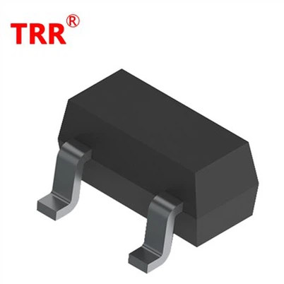
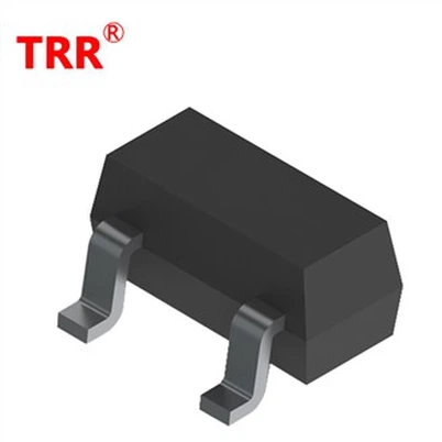
The core characteristic of a diode is to allow current to flow from the anode (A) to the cathode (K) while blocking in the opposite direction. After connecting a diode in series with the BMS power input terminal, when the power polarity is correct, the diode is in a forward conducting state, allowing current to pass through; When the power supply is reversed, the diode cuts off in reverse, directly blocking the current path.
Typical application cases:
The BMS control board of Tesla Model 3 adopts Schottky diode (SMA package, reverse withstand voltage 40V) as the anti reverse connection main device. This scheme utilizes the low forward voltage drop characteristic of Schottky diodes at around 0.3V, resulting in only 30W loss at 100A current, which is 40% more energy-efficient than ordinary diode schemes.
2. Collaborative protection of transient voltage suppression (TVS)
The simple diode scheme has two drawbacks:
Reverse withstand voltage limited (ordinary diodes usually<200V)
Unable to cope with transient high-voltage pulses
Therefore, the industry generally adopts a composite protection architecture of "TVS+diode":
TVS diode: parallel connected to the power input terminal, with a response time of<1ps, can clamp transient high voltage to a safe range in nanoseconds (such as SMCJ series can clamp 1000V pulse to 53.9V);
Anti reverse diode: series connected to the rear end of TVS, responsible for continuous reverse cutoff function.
Example of BMS design for a certain energy storage system:
In the 48V system, a 6600W TVS (clamp voltage 35.5V) packaged in DO-218AB is combined with a 400V voltage resistant diode. This scheme has passed the ISO7637 Pulse 5a test (generating a transient high voltage of 35V when the 12V system is unloaded), while meeting the requirement of a continuous reverse voltage of -100V.
三, Key technical parameters for device selection
1. Reverse Voltage Resistance (VRRM)
Must meet:
VRRM≥1.2×Vsystem_max
For example, in a 60V battery system, diodes with VRRM ≥ 72V should be selected. Automotive grade applications also need to consider the requirement of -14V continuous reverse voltage in ISO16750 standard.
2. Forward conduction voltage drop (VF)
In high current scenarios, VF directly affects system efficiency:
Ordinary silicon diode: 0.7-1.1V (loss reaches 70-110W at 100A)
Schottky diode: 0.2-0.5V (loss reduced by 60%)
Synchronous rectification MOS scheme:<0.1V (but requires complex driving circuit)
Industry data:
At a discharge current of 200A, using Schottky diodes can reduce 100W of heat loss compared to ordinary diodes, resulting in a 30% reduction in BMS heat dissipation design costs.
四, Industry Trends and Technological Evolution
1. Dispute over MOS tube replacement solutions
Although the PMOS anti reverse connection scheme has the advantage of zero voltage drop (the on resistance RDS (on) can be as low as 0.5m Ω), it has three major shortcomings:
Reverse withstand voltage limited (automotive grade PMOS typically<100V)
Higher cost (3-5 times higher than diodes of the same specification)
There is a voltage drop delay at the moment of disconnection
Actual measurement data:
A BMS test showed that when the power supply suddenly disconnects, the PMOS scheme causes the backend capacitor voltage to drop at a rate of 10V/ms, which may trigger a low voltage protection misoperation; The diode scheme can immediately cut off the circuit.
2. Fusion application of new devices
The industry is exploring the following innovative solutions:
SiC Schottky diode: voltage withstand increased to 650V, VF reduced to 0.8V, suitable for high-voltage fast charging scenarios;
Intelligent diode module: integrates reverse protection, over temperature detection, and status reporting functions, simplifying BMS design;
MEMS switch technology: using microelectromechanical systems to achieve lossless reverse blocking, but currently the cost is too high.
3. The Promoting Role of Standards and Regulations
ISO 26262 Functional Safety: Requires anti reverse circuits to have ASIL-B level redundancy design;
GB/T 38031-2021: It is explicitly required that BMS cut off the circuit within 1 second when connected in reverse;
UL 2580: It is stipulated that battery packs must have bidirectional current blocking capability.
五, Typical application scenario analysis
1. BMS for new energy vehicles
BYD blade battery BMS adopts three-level protection of "TVS+Schottky diode+self recovery fuse":
Level 1: 1500W TVS clamp transient high voltage
Second stage: 40V Schottky diode reverse cutoff
Level 3: PPTC implements overcurrent self recovery protection
This scheme has passed all pulse tests according to ISO7637, with a reverse protection response time of less than 50ns.
2. Energy storage system BMS
CATL's 48V energy storage BMS innovatively adopts a "back-to-back MOS+diode" hybrid solution:
Charging path: PMOS achieves zero voltage drop conduction
Discharge path: The diode provides reverse isolation
Cost optimization: Discharge MOS is replaced by diodes, reducing system costs by 18%
六, Technological challenges and development directions
The current industry is facing two core contradictions:
Balancing efficiency and safety: Low VF devices (such as GaN diodes) have high costs;
High voltage trend: The 800V platform requires protective devices to withstand voltage>1000V, while the maximum clamping voltage of existing TVS is only 660V.
Future technological development will focus on:
Large scale application of wide bandgap materials (SiC/GaN);
Digital protection technology (such as AI based fault prediction);
Standardized module design (such as protective IP cores that comply with AUTOSAR specifications).